How to Avoid Costly PCB Fabrication Mistakes - Essential PCB Layout Design Tips

Designing a reliable PCB starts long before the manufacturing process begins. At Bay Area Circuits, we’ve seen how small oversights in the early stages can lead to delays, redesigns, or even full production failures. By following a few essential PCB layout design best practices, you can avoid costly mistakes and ensure a smooth path from concept to production.
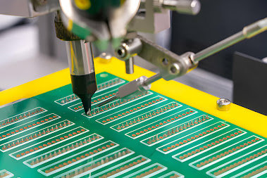
One common pitfall occurs when designers overlook spacing requirements. Inadequate trace width, tight component spacing, or insufficient copper clearance can lead to shorts or overheating during printed circuit board fabrication. Always reference IPC standards and your manufacturer’s guidelines to ensure optimal manufacturability.
Another area to watch is layer stack-up planning. Designers often finalize their layout before considering impedance control, copper balance, or thermal management. Proper stack-up ensures signal integrity and prevents warping during lamination.
When working on prototype PCB fabrication, communicate early with your fabrication partner. Sharing design files, confirming materials, and reviewing drilling or plating specifications reduces the chances of last-minute surprises. Early collaboration helps catch issues—such as unsupported vias or non-standard drill sizes—before they become costly problems.
To further streamline fabrication, always perform a thorough Design for Manufacturability (DFM) review. A simple check of silkscreen alignment, solder mask openings, and pad sizes can eliminate many common production issues.
By following these guidelines and partnering with a trusted domestic manufacturer like Bay Area Circuits, you can ensure your PCB moves through production efficiently and with fewer costly setbacks.
For more information read our blog now: https://bayareacircuits.notion.site/How-to-Avoid-Costly-PCB-Fabrication-Mistakes-Essential-PCB-Layout-Design-Tips-2bc4747f2941806091e0f09aaeea8b32
Comments
Post a Comment