Printed Circuit Boards Manufacturers & PCB testing Processes

Printed circuit board manufacturers are acutely aware of the importance of both testing and prototyping, and are increasingly leveraging data analytics to optimize these processes. This data-driven strategy enables PCB service providers to enhance quality standards while maintaining cost-effectiveness. How do they do this exactly? Read on to find out!
Prototype PCB fabrication & PCB design services
PCB designers never forget that even the smallest mistake within the layout of a printed circuit board can cascade into a much more significant issue, which has the potential to render an electronic product useless. A single routing issue, open connection, or incorrect component selection could cost thousands of dollars when you factor in wasted design and production time, product delays, and reputational damage.
Armed with this knowledge, printed circuit board manufacturers have developed sophisticated testing protocols that continually scan for potential issues from the PCB design services stage through to prototype PCB fabrication, and up to the packaging of the final product.
PCB testing has evolved dramatically over the past decade, thanks to the integration of automated systems capable of autonomously detecting defects measured in mere microns. The transformation from manual inspection and handling to fully automated systems reflects a multi-layered approach that begins with material inspection and handling.
The Flying Probe PCB Testing Method
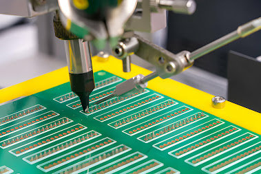
Bare Board Testing
PCB manufacturers employ several advanced electrical testing methods to stringently verify that every trace, via, and connection on the bare board is functioning as intended. ‘Flying probe’ testing is an advanced electrical testing method used to verify the electrical connectivity and functionality of circuit boards without requiring custom test fixtures. This method of testing is particularly suited to PCB prototyping and small-batch PCB production, as it does not require custom fixtures. It can therefore be rapidly adapted to accommodate various board designs.
The process employs multiple motorized probes that can move freely in three-axis directions over the surface of a PCB. These probes are controlled by a computer, allowing them to be precisely positioned at any point on the board. The probes then make temporary electrical contact to perform electrical measurements.
Key Features
Fixture-Free Testing: No expensive custom fixtures required for each PCB. Probes move to the necessary test points based on pre-programmed coordinates.
High Precision: Modern flying probe systems can achieve incredibly precise positioning with an accuracy of ±0.025 mm (±0.001 inch), allowing them to test even the smallest components and the most densely packed circuit board layouts.
Flexible Programming: Test programs can be quickly modified and updated without requiring changes to the hardware. That reduces production costs and time for small-scale PCB production and prototyping.
What does the Flying Probe Testing method detect?
Opens: Missing electrical connections where there should be continuity
Shorts: Unwanted electrical connections between different circuits
Resistance: Verification of resistor values and trace resistance
Capacitance: Testing of capacitor values and parasitic capacitance
Diode Testing: Forward and reverse bias characteristics
Basic Component Values: Verification of passive components
When Should PCB Designers and Manufacturers Employ Flying Probe Testing?
Prototype Development: Ideally suited to testing early-stage PCB designs
Small to Medium Scale Production: Cost-effective choice for limited runs where the cost of fixtures is prohibitive.
Complex Boards: Ideal for high-density interconnect boards, they have lots of small details
Mixed Technology PCBs: Suitable for boards that combine different technologies andorr components
Quick-Turn Services: Where time-to-market is crucial and fixture development has the potential to cause production delays
Comments
Post a Comment