How PCB Layout Design Impacts Signal Integrity and Product Reliability

You’ve probably had a piece of tech randomly glitch or shut down and you’re left wondering, “What just happened?” Well, sometimes, it all goes back to how the circuit board was designed. PCB layout design may sound like a behind-the-scenes task, but it has a significant impact on how electronics behave in the real world.
The design phase isn't just drawing lines.
When you think of circuit boards, you might picture a neat green slab with copper traces running like tiny highways. But laying out those traces isn't just about neatness, it’s about precision. If signals travel the wrong way, get delayed, or even interfere with each other, you’ll run into big problems. Think of audio interference, touchscreen lag, or dropped data. That’s what layout mistakes can cause.
What good layout design does
Let’s say you’re designing a smart home device. It’s compact, wireless, and relies on clean data transmission. The layout must accommodate antennas, filters, and processors—all without compromising signal integrity. If one trace overlaps where it shouldn’t, it could throw off the whole device. Clean layout design supports not just performance, but the long-term reliability of your product.
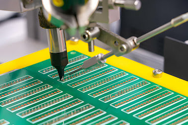
Why the manufacturer matters too
Here’s something most folks don’t think about: even if your layout is on point, your PCB manufacturing company has to build it the right way. Some designs look great on screen but don’t translate well to actual boards. Having designers and manufacturers working closely—ideally under the same roof—makes a big difference. It cuts back on surprises and gets you better boards faster.
It’s not all about fancy software.
Even the best PCB design services can’t fix everything if the foundation isn’t solid. That foundation? It’s the choices made early on—how components are placed, how power and ground planes are routed, and how the designer thinks ahead for manufacturing. It’s part art, part logic, and a bit of gut instinct (the good kind).
Takeaway? Think layout first
Whether you're building wearables, EV sensors, or industrial tools, the layout of your PCB is more than a visual—it’s the backbone of your product’s behavior. Skimping here can cause all kinds of headaches down the road. The good news? Some experts think about this stuff all day, so you don’t have to.
If you’re looking for design help that doesn’t miss the details, Bay Area Circuits is where we come in.
Comments
Post a Comment