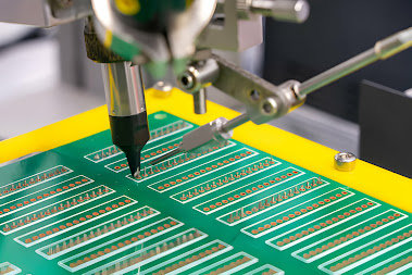
3 Best Practices in PCB Layout Design
Designing a printed circuit board (PCB) involves meticulous planning and a strong grasp of electrical engineering principles. Here are three best practices to elevate your PCB layout design:

Prioritize Your Board's Layout: Arrange components logically to minimize trace lengths and reduce the risk of signal interference. Ensure power and ground planes are properly positioned, with a solid ground plane under the signal layer to decrease electromagnetic interference, enhancing circuit stability.
Follow Design for Manufacturability (DFM) Guidelines: Adhering to DFM guidelines is essential for a seamless transition from design to physical production. These guidelines account for board size, layer count, trace widths, and via sizes, minimizing errors and revisions. This practice optimizes your PCB layout for manufacturing, leading to cost efficiency and quicker production.
Bay Area Circuits offers advanced printed circuit board design software like InstantDFM to optimize and validate your design. For high-quality printed circuit board fabrication, contact Bay Area Circuits for reliable and efficient services.
Design with Thermal Management in Mind: Proper thermal management is crucial to prevent overheating and performance degradation. Place heat-generating components apart, use thermal reliefs, and ensure adequate airflow around the board. To know more, Read this blog.
Comments
Post a Comment