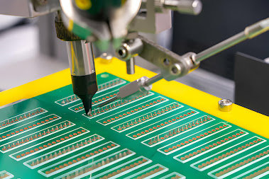
Advanced Techniques in PCB Layout Design
PCB layout design is a crucial aspect of electronics, requiring precision, knowledge, and creativity. Mastering component placement is the first step, where experienced designers prioritize minimizing routing complexity, ensuring signal integrity, and reducing electromagnetic interference. Components should be placed in the order of connectors, power circuits, sensitive circuits, critical signal routing, and other elements.
Ground and power planes are essential, acting as shields against electromagnetic interference, aiding heat dissipation, and ensuring a stable voltage supply. Using full-ground planes reduces loop areas and electromagnetic emissions, but designers should avoid splitting ground planes under high-speed signals to maintain integrity.
Trace routing should be short and direct, with serpentine traces maintaining signal integrity for longer paths. Differential pair routing, crucial for high-speed signals, involves routing two parallel traces to cancel out noise.
Design For Manufacturing (DFM) is vital for creating efficient and cost-effective PCB designs. DFM addresses component availability, solderability, and assembly processes during the design phase. Bay Area Circuits (BAC) offers tools like InstantDFM for customized PCB layouts and provides reliable prototype PCB fabrication services. Contact BAC for a quote today.
Originally Published at- https://bayareacircuits.notion.site/Advanced-Techniques-in-PCB-Layout-Design-3ed74977e3c7469dbc334228eda28db1

Comments
Post a Comment