How will future PCBs match the ever-increasing demands of the IT industry?
There has always been the question as to how PCBs can remain
relevant and meet the ever-evolving needs of the IT industry. We’ll look deeper
into this question in this article.
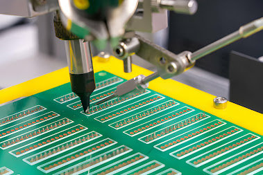
Prototype
printed circuit boards are getting smaller in size and now include more and
more components and wiring, in an effort to meet the demands of new
technologies and electronic products. To reach the required level of
miniaturization, circuitry density requires high-density interconnect (HDI).
The reduced trace widths & gaps required by HDI design, as well as the
utilization of even more components in a reduced space, will require both
material and manufacturing advancement.
A new generation of IT based on 5G technology with data
transmission rates of up to 52G, needs to transmit signals with high integrity
and minimal distortion on PCBs. Furthermore, the dielectric constant and
dielectric loss of PCB boards need to be kept to a minimum. All this means that
the epoxy resin-based substrate is barely able to keep up with the demands
placed on it. As a result, new resin-based substrates should be considered.
Information Technology (or IT), is a broad phrase that encompasses
all technologies engaged in the management and processing of data. PCBs
(Printed Circuit Boards) are at the heart of IT functioning, including
information production, information processing, data transport, and data
applications. The following features of a new generation of IT will be required
in the future: a new public telecommunication network, three-network integration,
IoT (Internet of Things), new flat panel displays, high-performance ICs, and
cloud computing. PCBs will naturally evolve as these increased demands are
placed on them.
The term "high performance PCB board" refers to a
board's increased durability and longevity. PCBs will always be integral to IT
evolution and there will always be further opportunity for improvement in the
manufacturing process too, as rising PCB complexity presents new hurdles to
manufacturers.
As a result, PCB
prototype manufacturers must make sure that PCBs not only perform well in
terms of density, signal transmission integrity, and thermal conductivity, but
also have a low CTE & a high tag. This will ensure that high-performance
PCBs are capable of being effective and dependable for the next generation of
IT.
To attain micro-sized PCBs, both material and fabrication
techniques must further be improved. In terms of substrate material, ultra-thin
copper foil can be used, which however does come at a premium cost and requires
a lengthy production process. As a result, the dominant development pathway is
to rely on copper foil thinning technology as a substrate material. PCB prototype
services are currently in high demand and this investment will give rise to
new PCB design and manufacturing processes in the future.
As the IT industry’s demands and priorities change, PCB
technologies will continue to evolve. One must keep a keen eye on changing
trends and develop new designs and invest in new technology. Furthermore, you
should team up with a PCB solutions provider that is ready to adapt to the
shifting technological demands.
Comments
Post a Comment